
Creating a circuit board is an essential skill for anyone interested in electronics, from hobbyists to aspiring engineers. This article will guide readers through the step-by-step process of designing and fabricating a circuit board, highlighting key tools and techniques along the way. Understanding how to make a circuit board not only empowers individuals to bring their ideas to life but also deepens their grasp of electrical engineering principles.
Overview of Circuit Boards
Circuit boards serve as the foundation for electronic devices, providing a platform for connecting electronic components. These boards primarily consist of a flat, rigid substrate, often made of fiberglass or composite materials, and have conductive pathways etched into their surface. These pathways allow electricity to flow between components like resistors, capacitors, and microcontrollers, enabling the device to function properly.
Types of circuit boards include:
- Printed Circuit Boards (PCBs): These are the most common type, featuring copper traces that form the electrical connections.
- Flexible Circuit Boards: These boards can bend and fold without breaking, making them suitable for compact devices.
- Rigid-Flex Circuit Boards: Combining flexibility and rigidity, these boards are used in applications where space and weight are critical.
- Multi-layered Boards: Composed of multiple layers, these boards can accommodate more complex circuits and components.
Understanding each type’s unique characteristics guides makers in selecting the right board for their projects. Circuit boards range in complexity from simple designs used in hobbyist projects to intricate architectures found in advanced electronics.
For those who prefer a professional approach, utilizing a pcb assembly service by OurPCB ensures high-quality results, especially for complex or large-scale projects.
Creating a circuit board is an essential skill for anyone interested in electronics. The design and fabrication processes improve knowledge of electronic principles and improve problem-solving capabilities within the field. These elements highlight the significance of mastering circuit board construction for both personal and professional development in electronics.
Essential Tools and Materials
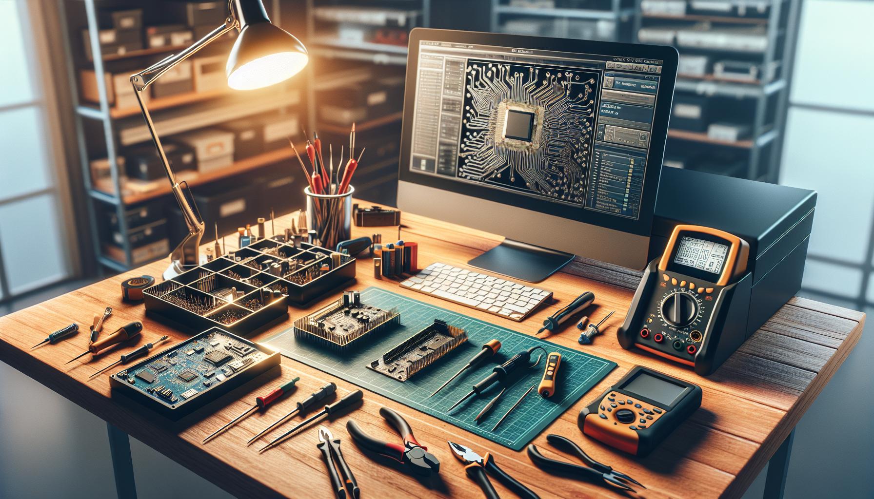
Creating a circuit board requires specific tools and materials that streamline the process. Below are the essential components needed for circuit board fabrication.
Tools Required
- Soldering Iron: A soldering iron enables precision when attaching components to the board.
- Wire Strippers: Wire strippers allow users to safely remove insulation from wires.
- Multimeter: A multimeter measures voltage, current, and resistance, essential for testing circuits.
- Drill: A drill provides the necessary holes for mounting components and enabling connections.
- PCB Design Software: PCB design software assists in layout creation, ensuring proper component placement.
- Etching Solution: An etching solution removes unwanted copper from the board during the fabrication process.
- Heat Gun: A heat gun helps in applying shrink tubing and other heat-sensitive materials.
Materials Needed
- Printed Circuit Board (PCB): PCBs serve as the foundation for electronic components over conductive paths.
- Solder: Solder connects components together and forms reliable electrical connections.
- Components: Resistors, capacitors, and integrated circuits are necessary for circuit functionality.
- Copper Foil: Copper foil provides conductive pathways on the circuit board.
- Masking Tape: Masking tape helps to shield areas of the board during etching.
- Adhesive: Adhesives secure components to the PCB, aiding in stability and durability.
Gathering these tools and materials ensures an efficient and effective workflow when creating circuit boards.
Designing Your Circuit Board
Designing a circuit board involves careful planning and execution through two main steps: schematic design and PCB layout design. Each stage plays a critical role in ensuring the functionality of the final product.
Schematic Design
Schematic design serves as the blueprint for the circuit board. It visually represents electronic components and their connections. To create effective schematics, use PCB design software like KiCad, Eagle, or Altium Designer. Follow these key practices for successful schematic design:
- Identify Components: List all components, including resistors, capacitors, and integrated circuits.
- Create Connections: Establish correct electrical connections between components using wires or nets.
- Label Components: Clearly label each component with its value and part number to avoid confusion.
- Check Errors: Validate the schematic using the software’s error-checking features to identify issues.
PCB Layout Design
PCB layout design translates the schematic into a physical representation for manufacturing. This step arranges components on the board and defines electrical pathways. Consider the following points during layout design:
- Arrange Components: Position components logically to minimize trace lengths and reduce interference.
- Route Traces: Connect components using copper traces while maintaining clearances. Keep high-frequency lines short.
- Define Ground and Power Planes: Utilize ground and power planes to ensure stable voltage levels and reduce noise.
- Review Design Rules: Follow manufacturing guidelines for trace widths, pad sizes, and hole dimensions to ensure manufacturability.
Through careful schematic and layout design, creators can develop functional and reliable circuit boards that meet project requirements.
Fabrication Process
The fabrication process of a circuit board involves several critical steps: printing the design, etching the board, and drilling and finishing the product. Each step demands precision for a successful outcome.
Printing the Design
Printing starts with transferring the PCB layout onto a transparent film. This film serves as a mask during the etching process. Designers print the layout using a laser printer for high-resolution images. After printing, they align the film over the copper-clad board, using a UV light exposure method if photoresist is applied. This exposure solidifies the exposed areas, preparing the board for etching by protecting the copper that remains covered.
Etching the Board
Etching removes unwanted copper from the PCB. The process involves immersing the board in an etching solution, typically ferric chloride or ammonium persulfate. The chemical reaction dissolves the exposed copper, leaving only the desired circuit traces intact. After etching, rinsing with water halts the etching process. Inspecting the board follows to ensure all unwanted copper has been removed, confirming the integrity of the circuit pattern.
Drilling and Finishing
Drilling involves creating holes for component leads and vias. Using a drill press or CNC machine, it’s crucial to drill accurately according to the layout specifications. After drilling, finishing steps include cleaning the board to remove debris and applying a surface finish, such as solder mask and silkscreen patterns. The solder mask insulates the copper traces, while the silkscreen provides labeling for components, enhancing the board’s functionality and readability.
Assembly of Components
Assembling components accurately ensures circuit board functionality. This section outlines essential soldering techniques and testing methods for effective assembly.
Soldering Techniques
Soldering techniques play a crucial role in assembling circuit boards. Users typically follow these steps:
- Prepare the Work Area: Keep the workspace clean and organized to avoid accidents.
- Heat the Soldering Iron: Allow the iron to reach the appropriate temperature, usually between 350-400°C (662-752°F).
- Tin the Tip: Apply solder to the iron tip before use for better heat transfer.
- Insert Component Leads: Push component leads through designated holes in the PCB.
- Heat and Apply Solder: Position the soldering iron on the lead and pad simultaneously. After heating, apply solder, ensuring it flows around the joint.
- Inspect the Joint: Verify that the joint is smooth and shiny, indicating a good connection.
- Trim Excess Leads: Use wire cutters to trim any excess lead length for a neater finish.
These techniques improve the stability of components on the circuit board and prevent issues like cold solder joints.
Testing Your Circuit Board
Testing the circuit board confirms its proper functionality. Follow these steps for effective testing:
- Visual Inspection: Check for solder bridges, missing components, or damaged traces.
- Use a Multimeter: Measure resistance, continuity, and voltage at different points in the circuit.
- Power Up the Board: After visual checks, apply power and monitor behavior.
- Test with an Oscilloscope: Examine signal integrity and timing if applicable.
- Check All Connections: Ensure the connections meet specific voltage levels and operate as intended.
Performing these tests ensures that the circuit board operates correctly, leading to successful project completion.
Conclusion
Mastering the art of circuit board creation opens doors to a deeper understanding of electronics. With the right tools and techniques, anyone can transform their ideas into functional designs. The journey from schematic to assembly not only enhances technical skills but also fosters creativity.
Whether a hobbyist or an aspiring engineer, the ability to design and fabricate circuit boards is invaluable. It empowers individuals to tackle complex projects and innovate in the field of electronics. Embracing this skill leads to personal growth and professional opportunities. As technology continues to evolve, the demand for knowledgeable creators will only increase.
Frequently Asked Questions
What are circuit boards and why are they important?
Circuit boards serve as the foundation for electronic devices, connecting various components through conductive pathways. They are crucial for hobbyists and engineers to realize their ideas and deepen their understanding of electrical engineering principles.
What types of circuit boards exist?
The main types include Printed Circuit Boards (PCBs), Flexible Circuit Boards, Rigid-Flex Circuit Boards, and Multi-layered Boards. Each type has unique characteristics suitable for different applications, helping creators select the right one for their projects.
What tools do I need to create a circuit board?
Essential tools include a soldering iron, wire strippers, a multimeter, a drill, PCB design software, an etching solution, and a heat gun. These tools facilitate an efficient workflow during the design and fabrication of circuit boards.
What are the main steps in the circuit board design process?
The design process consists of two main steps: schematic design and PCB layout design. Schematic design visually represents components and connections, while PCB layout design translates this into a physical representation for manufacturing.
How do I fabricate a circuit board?
The fabrication process involves printing the design, etching the board, and drilling it. First, transfer the design onto a film, etch the board to remove unwanted copper, drill holes for components, and complete finishing steps for usability.
What soldering techniques should I know for assembling components?
Important soldering techniques include preparing your workspace, heating the soldering iron, tinning the tip, inserting component leads, applying solder, inspecting joints, and trimming excess leads. These techniques are crucial for creating stable electrical connections.
How do I test the functionality of my circuit board?
Testing involves visual inspection, using a multimeter, powering up the board, testing with an oscilloscope, and checking all connections. Performing these tests ensures your circuit board functions correctly, leading to successful project completion.